Accumulator Shifting Unit 2
Accumulator
Main Adder
Computer Control I
Computer Control X
Computer Control II
Computer Control III
Computer Control IV
Computer Control V
Computer Control VI
Computer Control VII
Computer Control VIII
Computer Control IX
Coincidence Unit
Clock Generator
Complementer/Collater
Control Switches and Logic
Counter
Digit Pulse Generators
Engineers Control Panel
Frigs
Half Adder Type 1
Half Adder Type 2
Main Control Unit
Multiplicand Tank
Memory Units
Multiplier Tank
Order Coder
Order Decoder 1
Order Decoder 2
Order Flashing Unit
Order Tank
Printer
Sequence Control Tank
Initial Orders Loader
Timing Control Tank
Tank Address Decoder 0
Tank Address Decoder 1
Tank Address Distribution
Tank Address Flashing Units
Tank Address Decoding Final Stage
Tape Reader
Test Frigs
Transfer Unit
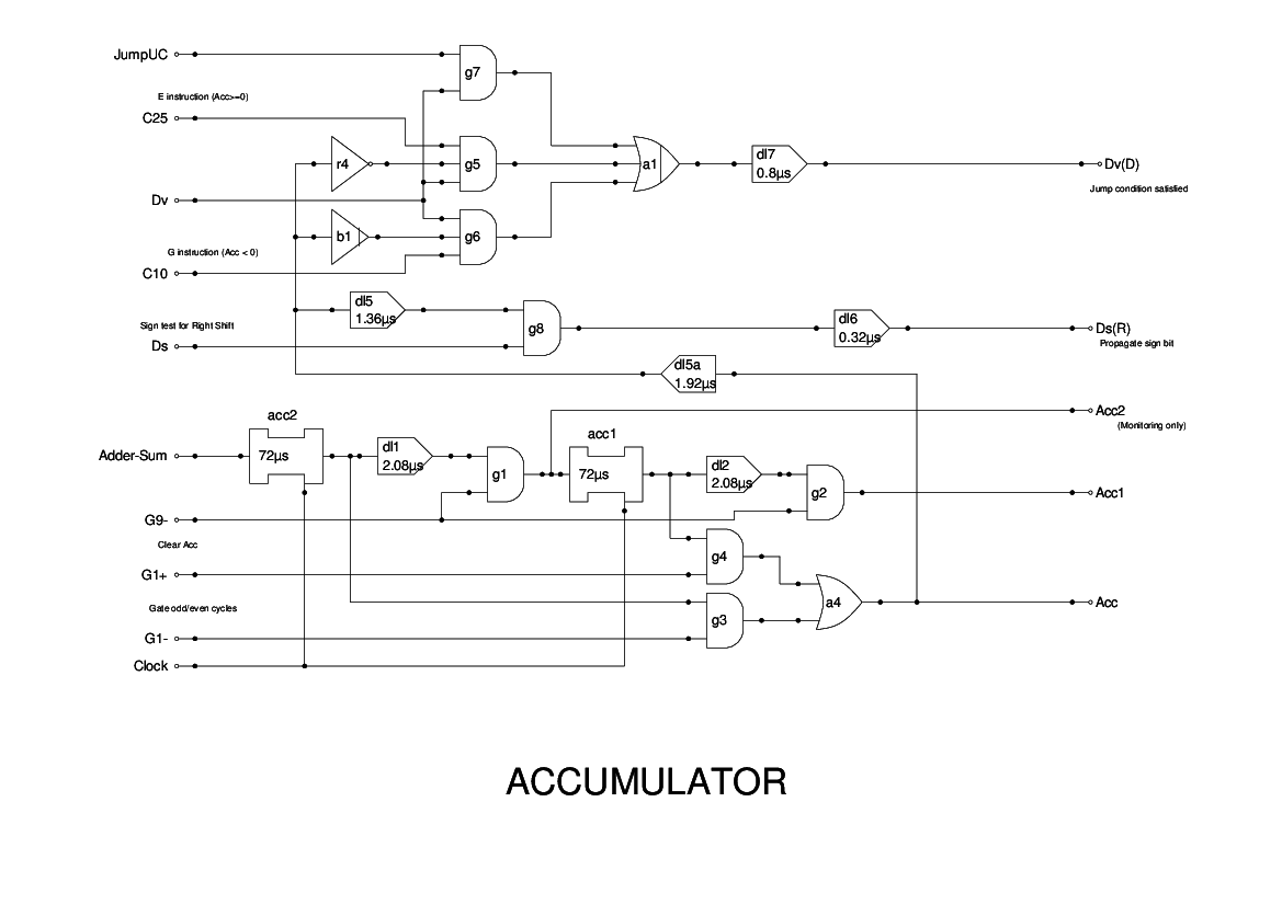
This is the Accumulator and associated logic. In order to handle multiplication of two 35-bit numbers, the Accumulator is double length and consists primarily of two delay tanks. One (Acc1) is 36 bits in length, the other (Acc2) is 4 bits shorter as the content is re-circulated via the shifting unit (2 bits delay) and the Adder (2 bits delay).
In order to adjust the timing under the simulator I have had to split these two tanks into sections so that an earlier output can be obtained and fed out to the memory units. This is unfortunate, but at least it works. I do have concerns about logic delays but some experiments have been made and it seems that the delays are likely to be much less in practice.
The logic here is substantially more than can be accomodated by a single panel, but as we have no indication (yet) as to where the split should be I have simply fitted it all into one module.
The top section is the main accumulator tanks and gating. Below this is some logic for testing the sign of the Accumulator. This tests bit 35 of the number, which is a one if the number is negative.
Below this is some gating to control when the Accumulator is fed out via the Output Bus (MOB) during store instructions. The gate g10 inhibits the output at bit 0 and bit 18 (for short instructions).
The bottom section should really be associated with the Shifting Unit, but was shown lumped with the output gating on original drawings. These gates are used to control the Shifting Unit when shift operations are issued.
The top half of this diagram is my own reconstruction. Apart from textual references to the Accumulator in the Report, there are no figures illustrating this, down to where the signal Ds comes in at the left. The remaining section is shown as Figure 10(a) as ASU I.
I have had to adjust the delays a little to reconcile things with my simulator. DL4 is specified as 1PI in the Report but has been shortened to compensate for the extra delays incurred by my simulator.