Accumulator Shifting Unit 2
Accumulator
Main Adder
Computer Control I
Computer Control X
Computer Control II
Computer Control III
Computer Control IV
Computer Control V
Computer Control VI
Computer Control VII
Computer Control VIII
Computer Control IX
Coincidence Unit
Clock Generator
Complementer/Collater
Control Switches and Logic
Counter
Digit Pulse Generators
Engineers Control Panel
Frigs
Half Adder Type 1
Half Adder Type 2
Main Control Unit
Multiplicand Tank
Memory Units
Multiplier Tank
Order Coder
Order Decoder 1
Order Decoder 2
Order Flashing Unit
Order Tank
Printer
Sequence Control Tank
Initial Orders Loader
Timing Control Tank
Tank Address Decoder 0
Tank Address Decoder 1
Tank Address Distribution
Tank Address Flashing Units
Tank Address Decoding Final Stage
Tape Reader
Test Frigs
Transfer Unit
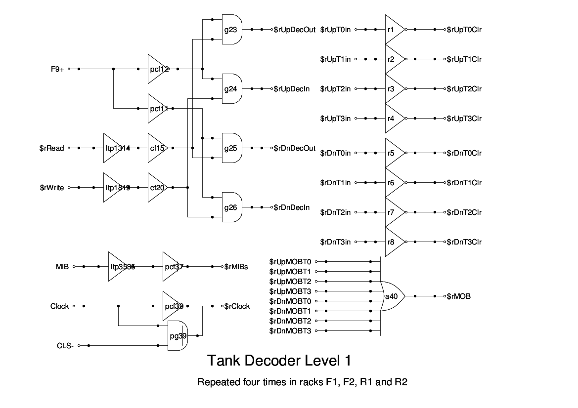
This drawing shows the second level of decoding. This panel is replicated on each of the four memory racks and takes the control signals provided by the first level decoder, along with bit 9 (F9) of the order, to select one of the final decoders. These are duplicated on each memory rack and are designated Up and Down.
The gates at the upper left portion perform this decoding generating four control signals DecUpOut, DecUpIn, DecDownOut and DecDownIn.
In addition, the panel also contains buffers and inverters:
At bottom left two buffers provide Main Input Bus (MIB) and Clock signals to each of the Memory Panels.
At upper right are eight inverters which invert the input gating signals (T0In - T7In) to close off the recirculation path in the Memory Panels when new data is being written to memory.
Finally, at bottom right is an eight-input wired-OR gate which merges and buffers the outputs from the Memory Panels to feed the Main Output Bus (MOB0).